Silicon IP Cores
R8051XC2
High-Performance, Configurable, 8-bit Microcontroller
The R8051XC2 configurable processor core implements a range of fast, 8-bit, micro-controllers that execute the MCS®51 instruction set.
The IP core runs with a single clock per machine cycle, and requires an average of 2.12 machine cycles per instruction. Dhrystone 2.1 tests show it to run from 9.4 to 12.1 times faster than the original 8051 at the same frequency. Representative 40 nm ASIC results have reached 1.2 GHz, for an effective speed up of 1,200 times over 80C51 chips.
The core has a rich set of optional features and peripherals. Designers can choose from several versions, including the easy-to-configure full version with all options included; a custom, non-configurable version with options specified at purchase; and pre-packaged versions with different sets of options and degrees of configurability.
All versions of the core benefit from power-saving architectural efficiency—the R8051XC2 is 10% better in milliwatts/DMIP than our previous generation—and various power-management options are available. System development is facilitated through a native on-chip debugging option and support by development tools from Keil and IAR.
This product builds on CAST’s experience with hundreds of 8051 IP customers going back to 1997. Designed for easy reuse in ASICs or FPGAs, the core is strictly synchronous, with positive-edge clocking (except in the optional debug & SPI modules), synchronous reset, and no internal tri-states. Representative 65nm ASIC results show the core to be conservative in its use of space, requiring just 7,900 to 30,000 gates (DMA not included).
The core’s architecture eliminates redundant bus states and implements parallel processing of fetch and execution phases. Since a cycle is aligned with memory fetch when possible, most of the 1-byte instructions are performed in a single cycle.
The core uses one clock per cycle. This, together with other extensions (multi-DPTR, MDU), leads to significant performance improvements with respect to the original Intel device operating with the same clock frequency.
The Dhrystone 2.1 benchmark score varies from 0.088 to 0.114 DMIPS/MHz, which translates to speed improvements from 9.4 to 12.1 times over the standard 80C51, or 1200 times the maximum performance at 1.2 GHz in 40nm technology.
Sample Dhrystone 2.1 benchmark results are as follows.
|
Configuration |
DMIPS/MHz |
80C51 Speed Ratio |
|
Basic |
0.0883 |
9.4 |
|
Multiple DPTR |
0.1020 |
10.9 |
|
Multiple DPTR+auto-inc |
0.1111 |
11.8 |
|
MDU+Multiple DPTR+auto-inc |
0.1136 |
12.1 |
Preconfigured Versions
Three standard core versions of the core are available, offering a range of capabilities and prices.
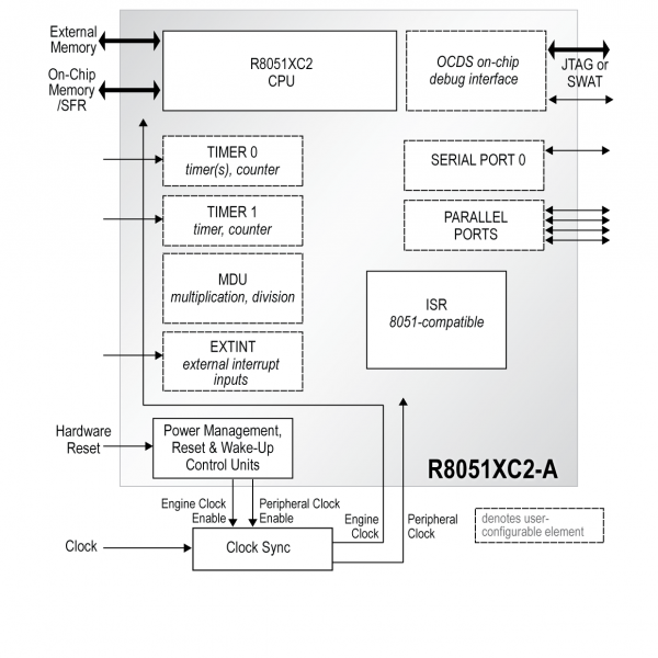
- R8051XC2-A includes options that match the original Intel 8051 peripheral set: 64kB memory interface, two timers, one serial port, four parallel I/O Ports, two-level interrupt controller, and two DPTR registers. These options are user-configurable (i.e., may be deleted prior to synthesis).
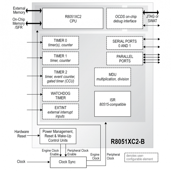
- R8051XC2-B includes options that match the Infineon 80515/80517 peripheral set: 64kB memory interface, three timers, two serial ports, four parallel I/O ports, watchdog timer, multiplication-division unit, and two DPTR registers. These options are user-configurable (i.e., may be deleted prior to synthesis).
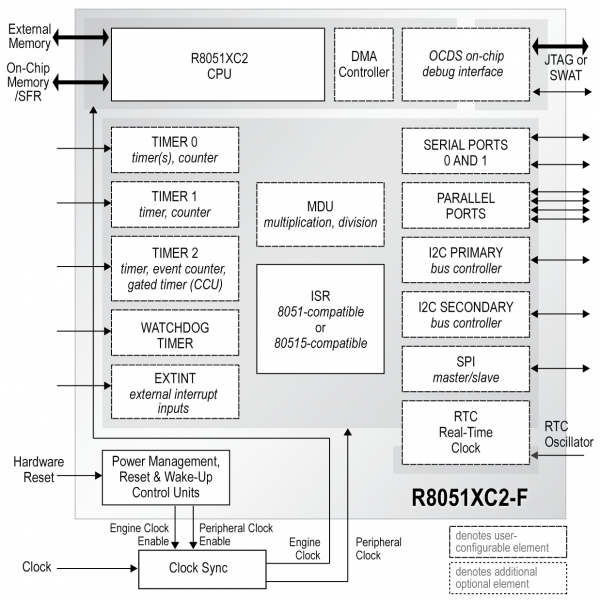
- R8051XC2-F includes the full set of options, and is user-configurable (i.e., options may be included or excluded prior to synthesis).
ASIC (RTL) and FPGA (netlist) deliverables are available; FPGA packages are not user-configurable.
The native debugging package is an extra option for all versions.
The core has been verified through extensive synthesis, place and route, and simulation runs. It has been embedded in numerous shipping customer products, and is proven in both ASIC and FPGA technologies.
The core is available in ASIC (synthesizable HDL) or FPGA (netlist) forms, and includes everything required for successful implementation. ASIC versions include:
- HDL RTL source code
- Easy-to-use configuration tool (with configurable versions)
- An example chip implementation, which uses the core in a sample system
- Sophisticated self-checking HDL Testbench including everything needed to test the core (Verilog versions use Verilog 2001)
- Simulation script, vectors, and expected results
- Synthesis script
- Comprehensive user documentation, including detailed specifications and a system integration guide
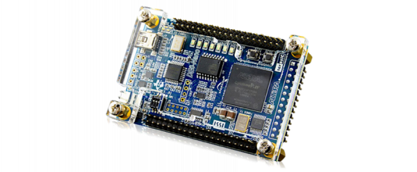
- A reference design board is available; contact CAST Sales for information
R8051XC2 designs have been evaluated in a variety of technologies. The following are sample ASIC pre-layout results reported from synthesis with a silicon vendor design kit under typical conditions, with all core I/Os assumed to be routed onchip.
| Configuration | Technology | Area (EQ. Gates) | Freq (MHz) |
|---|---|---|---|
| R8051XC2 (CPU - Only) | TSMC 65nm | 7,900 | 100 |
| R8051XC2-A | TSMC 65nm | 12,100 | 100 |
| R8051XC2-B | TSMC 65nm | 19,600 | 100 |
| R8051XC2-F | TSMC 65nm | 30,000 | 100 |
| R8051XC2 (CPU - Only) | TSMC 16nm | 7,300 | 300 |
| R8051XC2-A | TSMC 16nm | 10,900 | 300 |
| R8051XC2-B | TSMC 16nm | 18,000 | 300 |
| R8051XC2-F | TSMC 16nm | 27,000 | 300 |
The DMA requires an additional 3.5K gates. Each additional channel requires 2K gates.
OCDS requires an additional 4K gates for 2 hardware break-points.
The provided figures do not represent the higher speed or smaller area for the core and area figures do not include any memories.
Features List
- Fully compatible with the MCS® 51 instruction set
- Single clock per cycle and efficient architecture for up to 12.1 times the performance of original 8051
- Fewer machine cycles means lower average power usage in most applications
- Extensive set of optional features and peripherals
- JTAG-based On-Chip Debug Support (OCDS) or single-wire Debug (SWAT)
- Integrated with IAR Embedded Workbench & Keil uVision™ IDEs
Options and Peripherals
Full user-configurable version includes all of these; other versions include a subset (see Versions).
- External Memory Interface:
- Addresses up to 8 MB of Program and Data Memory each
- One, two or eight Data Pointers for fast data block transfer
- Additional Arithmetic Unit supports data pointers, auto-increment/-decrement, and auto-switch
- Supports external DMA controller through HOLD function
- Program memory write mode
- Multiplication-Division Unit
- 36 to 119 external Special Function Registers
- Interrupt Controller with two or four priority levels, and six or eighteen interrupt sources
- Up to six Parallel I/O Ports
- Serial 0 full-duplex serial interface (80C51-like), equipped with an additional baud rate generator
- Serial 1 interface: an asynchronous-only version of Serial 0
- SPI Master/Slave interface
- One or two I2C™ Master/Slave interfaces
- Timers 0, 1 and Timer 2 with Compare/Capture (80C515-like)
- 15-bit programmable Watchdog Timer
- Real Time Clock
- Direct Memory Access (DMA) Controller
- Power Management Unit with power-down modes (IDLE/STOP)
- Bridges for integrating with APB, AHB-Lite, or AXI4-Lite peripherals available upon request
Resources
Development Tools & Options
Code and debug this 8051 with these popular IDEs:
IAR Systems Embedded Workbench for 8051
These tools work with an optional, native on-chip debug block and inexpensive external adapter (pod) with a JTAG four-wire or SWAT Single-Wire PC interface.
Evaluation: Try it for Yourself
Easily evaluate this 8051's features and performance in your own environment with the
Talos Series Evaluation Kit for 8051s.
Articles
Understanding Interrupt Latency in Modern 8051s
by Nikos Zervas at ChipEstimate.com


