Silicon IP Cores
MM2ST
AHB/AXI4-Lite to AXI4-Stream Bridge
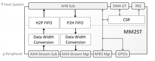
The MM2ST IP core bridges the streaming interfaces of a peripheral or accelerator to a memory-mapped AMBA® AHB or AXI4-Lite bus.
The MM2ST core is rigorously verified, LINT-clean, and scan-ready. It is available in synthesizable Verilog and FPGA netlist forms and ships with everything required for successful implementation, including a testbench, simulation, and synthesis scripts, and comprehensive user documentation.
The MM2ST core can be used in any SoC integrating streaming-capable peripherals that need to receive input or store outputs via a memory-mapped bus. Examples include compression, video, or packet processing engines. The core is an excellent companion to CAST’s data compression, video or image codecs, IP stacks, or cryptography cores
The MM2ST as delivered is warranted against defects for ninety days from purchase. Thirty days of phone and email technical support are included, starting with the first interaction. Additional maintenance and support options are available.
The MM2ST core is a purely digital design and can be mapped to any standard cell technology. The following table provides sample implementation results for the core constrained to 0.5GHz, synthesized on a TSMC 7nm technology.
|
Configuration |
Logic Resources (Eq. Gates) |
Memory Resources |
|---|---|---|
|
32-bit AHB, 16-bit AXI4-Stream P2H & H2P, 32 GPIOs, 8-words deep CDC FIFOs and 16-words deep data FIFOs |
9,210 |
1,712 |
|
32-bit AHB, 32-bit AXI4-Stream P2H & H2P, 64 GPIOs, 8-words deep CDC FIFOs and 16-words deep data FIFOs |
7,753 |
1,712 |
|
32-bit AHB, 256-bit AXI4-Stream P2H & H2P, 64 GPIOs, 8-words deep CDC FIFOs and 256-words deep data FIFOs |
18,225 |
18,752 |
These sample implementation figures do not represent the highest speed or smallest area possible for the core. Please contact CAST to discuss silicon resource utilization and performance for your target configuration and technology.
The MM2ST core is a purely digital design and can be mapped to any Altera FPGA. The following table provides sample implementation results for an Arria1-GX device and all clocks constrained to 300MHz.
|
Configuration |
Logic Resources (ALMs) |
Memory Resources (Block Mem. bits) |
|---|---|---|
|
32-bit AHB, 16-bit AXI4-Stream P2H & H2P, 32 GPIOs, 8-words deep CDC FIFOs and 16-words deep data FIFOs |
690 |
1,712 |
|
32-bit AHB, 32-bit AXI4-Stream P2H & H2P, 64 GPIOs, 8-words deep CDC FIFOs and 16-words deep data FIFOs |
680 |
1,712 |
|
32-bit AHB, 256-bit AXI4-Stream P2H & H2P, 64 GPIOs, 8-words deep CDC FIFOs and 256-words deep data FIFOs |
1,268 |
18,752 |
These sample implementation figures do not represent the highest speed or smallest area possible for the core. Please contact CAST to discuss silicon resource utilization and performance for your target configuration and technology.
The MM2ST core is a purely digital design and can be mapped to AMD FPGA. The following table provides sample implementation results for an Artix UltraScale+ device with all clocks constrained to 300MHz.
|
Configuration |
Logic Resources (LUTs) |
Memory Resources (RAMB18) |
|---|---|---|
|
32-bit AHB, 16-bit AXI4-Stream P2H & H2P, 32 GPIOs, 8-words deep CDC FIFOs and 16-words deep data FIFOs |
744 |
0 |
|
32-bit AHB, 32-bit AXI4-Stream P2H & H2P, 64 GPIOs, 8-words deep CDC FIFOs and 16-words deep data FIFOs |
691 |
0 |
|
32-bit AHB, 256-bit AXI4-Stream P2H & H2P, 64 GPIOs, 8-words deep CDC FIFOs and 256-words deep data FIFOs |
1,098 |
2 |
These sample implementation figures do not represent the highest speed or smallest area possible for the core. Please contact CAST to discuss silicon resource utilization and performance for your target configuration and technology.
Features List
Memory-Mapped to Stream Bridge
- Bridges AXI4-Stream and APB register interfaces of a peripheral to a 32-bit or 64-bit AHB or AXI-Lite subordinate port
- Optionally implements clean CDC boundaries between the pe-ripheral and the host bus clocks
- Performs data-width conversion from/to the peripheral’s buses data widths to/from the width of the memory mapped bus
Interfaces
- Host Interface:
- 32-bit or 64-bit AHB or AXI4-Lite Subordinate
- Interrupt with maskable sources
- Peripheral Interface
- A configurable-width (up to 512 bits) AXI4-stream per direction
- 32-bit APB interface for CSR access
- Configurable number of GPIOs
- Handshaking signals for external DMA controller
Synthesis-Time Configuration Options
- Data width for the AXI-Stream interfaces
- Data width of the memory-mapped interface (32 or 64 bits)
- Number of general-purpose in-put and output pins
- AHB address width
- Instantiation of the APB manager port
- APB address offset and width
- Instantiation of CDC logic
- FIFO sizes
Deliverables
- Synthesizable RTL or FPGA netlist
- Verilog testbench & sample test cases
- Simulation & synthesis scripts
- Documentation

